


")
")
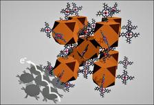
Three-dimensional lattice of nanocrystals and semiconducting molecules. The precise arrangement of the nanocrystals allows current in the form of electrons (e-) to flow in certain directions. (Illustration: University of Tübingen, Andre Maier)
Electronic components such as light-emitting diodes or solar cells can never be too minute. The smaller they are, the less power they consume and the wider the range of possible applications. In order to explore smaller and smaller worlds, scientists are constantly on the lookout for new materials with interesting properties. A research team from the University of Tübingen, working with colleagues at DESY and from Russia, has now made such a discovery. It is reporting its findings in the journal Advanced Materials.
The scientists attached semiconducting organic molecules to inorganic nanocrystals to form ordered, three-dimensional lattices that have a uniform superstructure and are electrical conductors. “For the first time ever, we were able to determine a correlation between the conductivity and the direction of electrical transport in such lattices made up of nanocrystals,” said Marcus Scheele from the University of Tübingen, one of the team’s two leaders, adding that this is hugely significant in terms of their use in electronic components.
“I was fascinated by the great structural diversity that can be observed when large numbers of inorganic nanocrystals are made to arrange themselves in a periodic pattern as a mesocrystal,” says Andre Maier, Scheele’s university colleague and the principal author of the study. “For more than 25 years, it has been known that such nanocrystals could be arranged in highly ordered structures like this,” reports Scheele, “but until now, no benefits had been identified.”
It took many years of close collaboration between the chemistry and physics departments at the University of Tübingen and DESY to bring about a shift in this perception. “At Tübingen, the core facility LISA+ provided the necessary infrastructure to perform the various lithographic procedures, to measure the electrical transport and to carry out X-ray scattering experiments at the highest level,” Scheele notes. “The question was ideal from our point of view, to fully exploit the strengths of the P10 coherence beamline at PETRA III together with the X-ray cross-correlation analysis we operate,” adds DESY’s Ivan Vartanyants, the second leader behind the study.
“PETRA III is a storage-ring-based X-ray source with a high spatial resolution, allowing us to determine the local structure of the mesocrystals to within a few hundred nanometres. That is what led to the breakthrough,” explains Maier. The research team proved for the first time that conducting mesocrystals made up of lead sulphide nanoparticles display directional transport behaviour. “This is otherwise only found in a small number of materials, such as graphene or black phosphorus,” explains Scheele.
The University of Tübingen, the Russian National Research Nuclear University (MEPhI) in Moscow, the Russian National Research Tomsk Polytechnic University (TPU) and DESY participated in the study.
(from DESY News)
Reference:
Structure-Transport Correlation Reveals Anisotropic Charge Transport in Coupled PbS Nanocrystal Superlattices; Andre Maier, Dmitry Lapkin, Nastasia Mukharamova, Philipp Frech, Dameli Assalauova, Alexandr Ignatenko, Ruslan Khubbutdinov, Sergey Lazarev, Michael Sprung, Florian Laible, Ronny Löffler, Nicolas Previdi, Annika Bräuer, Thomas Günkel, Monika Fleischer, Frank Schreiber, Ivan A. Vartanyants, Marcus Scheele; „Advanced Materials“, 2020, DOI: 10.1002/adma.202002254