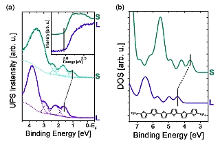
Figure 1: (a) Experimental valence band spectra for 4 Å of DH6T (wine), and 40 Å of DH6T (olive) on Ag(111), corresponding to a lying monolayer (L) and a second standing layer (S). The dotted lines indicate the least-squares fit to determine the peak positions. The inset shows the secondary electron cut-offs used to determine the work function of the respective sample. (b) DFT calculated density-of-states (DOS) of a single layer of lying (wine) and standing (olive) DH6T molecules; the zero of the energy scale is the vacuum level.

Steffen Duhm1, Georg Heimel1, Ingo Salzmann1, Hendrik Glowatzki1, Robert L. Johnson2, Antje Vollmer3, Jürgen P. Rabe1, and Norbert Koch1
1Institut für Physik, Humboldt-Universität zu Berlin, Newtonstr. 15, D-12489 Berlin, Germany
2Institut für Experimentalphysik, Universität Hamburg, D-22761 Hamburg, Germany
3Berliner Elektronenspeicherring-Gesellschaft für Synchrotronstrahlung m.b.H., D-12489 Berlin, Germany
Published as: “Orientation-dependent ionization energies and interface dipoles in ordered molecular assemblies”, Nature Materials 7, 326 - 332 (2008)
Organic molecules provide fascinating possibilities for fabricating inexpensive novel electronic devices, organic light-emitting diodes, and flexible environmentally-friendly low-cost solar cells [1]. The efficiency of organic solar cells depends on the chemistry of the materials employed and critically on the electronic properties and nanomorphology of the molecules in the active layer [2]. We have used synchrotron light at HASYLAB to investigate how the orientation of the organic molecules in thin films affects the electronic structure [3].
The work function of a metal is defi ned as the energy difference between the Fermi level (EF) and the vacuum level (Vvac) and depends on the crystallographic orientation of the surface. For van der Waals crystals of non-dipolar molecules, surface dipoles and work-function anisotropy have yet to be investigated systematically. In the past variations in the ionization potential (IP; the molecular equivalent of the work function) with molecular orientation were interpreted in terms of variable photohole screening [4], but could never be quantified satisfactorily. Here, we propose a novel explanation of the intriguing observation that one and the same molecule can have different, yet still well-defined, ionization potentials if it forms part of an ordered supramolecular structure.
We performed photoelectron spectroscopy investigations on α,ω-dihexyl-sexithiophene (DH6T) and α-sexithiophene (6T), deposited on Ag(111) substrates at the FLIPPER II beamline. The ionization potentials of the molecules change by up to 0.6 eV, depending on whether they are lying flat on the substrate, or standing upright. We explain these observations in terms of the collective electrostatic effect of the highly anisotropic intra-molecular charge distribution based on density-functional theory (DFT) calculations and electrostatic modelling. Supplementary studies on different substrates and molecules underline the universality of the observed effects and their explanation. We stress that the general concept is also valid for single crystals and ordered polymers.
The valence band spectra for DH6T on Ag(111) in the monolayer (L for „lying“) and multilayer (S for „standing“) regimes are shown in Figure 1a, and the corresponding simulated spectra from density functional theory (DFT) are shown in Figure 1b. Three low binding energy (BE) peaks can be clearly distinguished with maxima at 1.6 eV, 2.3 eV, and 2.9 eV in the L-regime, and at 1.0 eV, 1.7 eV, and 2.3 eV in the S-regime. These peaks are derived from the highest occupied molecular orbital (HOMO).
All peaks are at 0.6 eV lower BE for the (standing) multilayer (S) compared to the (lying) monolayer (L). The change in the intensity ratio of the fi rst two peaks arises from the different orientations of the molecular axes. The -0.6 eV binding energy shift of the molecular levels directly translates into a reduction of the molecular IP (i.e., the energy difference between HOMO and Vvac).
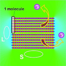
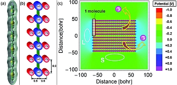
Figure 2: Electrostatic modelling of the orientation-dependent ionization potential. The electron density of a single 6T molecule (a), is approximated by a model molecule consisting of a series of point charges (b) (distances and charges are given in atomic units). (c) Electrostatic potential in and around a model molecular crystal consisting of two layers of 21 model-molecules.
While DFT calculations permit a quantitative analysis (Fig. 1b), an even simpler, purely electrostatic model can be used to provide a more intuitive picture. We approximate the charge distribution corresponding to one 6T molecule (the conjugated
core of DH6T; Figure 2a) by a number of point-charges (Figure 2b): The π-electron system above and below each ring is clearly negatively charged; this is represented by negative point charges of -0.5 e (elementary charge) placed 0.5 bohr above and below the molecular plane. These negative charges are compensated by a +1.0 e point charge in the plane of the molecule. This pattern is repeated six times (one for each ring) along the long molecular axis with a spacing of 8 bohr (≈ distance between individual thiophene rings). Next a 2D molecular crystal is built using this model molecule (Figure 2c), consisting of 21 standing model-molecules in one layer with a distance of 6 bohr between the long molecular axes with a second layer placed under the first layer with a 10 bohr gap.
This model-crystal has two distinctly different crystal faces: the top and bottom are terminated by the point-charge pattern - 0.5|+1.0|-0.5||-0.5|+1.0|-0.5||… given by the hydrogen-terminated ends of the 6T molecules exposed in a standing layer; the left and right faces are terminated by negatively charged sheets that represent the π-electron cloud exposed in a lying layer. The electrostatic potentials of all point charges are summed to yield the potential within and around the model-crystal (shown in colour in Figure 2c). In analogy to the results from the DFT calculations, we find an extended region of lower electrostatic potential (green) over the hydrogen-terminated ends of the molecules, relevant for the standing layer (S). Above the π-system,
there is an extended region of higher electrostatic potential (cyan), relevant for the lying layer (L). As a consequence, the work required to promote an electron from any energy level within the crystal into the region above the hydrogen-terminated ends (S) is less than that for promoting an electron into the region above the π-electron clouds (L). This difference can be measured provided the lateral extent of the supramolecular structure is large compared to a single molecule.
We have shown that pre-patterning of a metal surface with an appropriate molecular species is a promising tool for controlling the orientation of subsequently deposited molecules. Since the charge-carrier mobility and photoluminescence depend on the orientation of the intrinsically anisotropic molecules our findings will lead to improved organic electronic devices.
|
References |
||||||||
|
||||||||
|
Contact information |
||||||||
|
Norbert Koch |
||||||||
| Further Information |


