


")
")

Figure 1: (a) X-ray reflectivity curves of the sample (the x-axis increments are chosen to match the 00L peak series of pentacene) and (b) reciprocal space map of the same sample. (c) Atomic force microscope (AFM) amplitude image of a 50 nm thick TTC layer on a 50 nm pentacene thin film.
Martin Göllner, Martin Huth, Bert Nickel
Fakultät für Physik & CeNS, Ludwig-Maximilians-Universität, Geschwister-Scholl-Platz 1, 80539 München, Germany
Published as: “Pentacene Thin-Film Transistors Encapsulated by a Thin Alkane Layer Operated in an Aqueous Ionic Environment”, Advanced Materials 22, 4350–4354 (2010). Letters 105, 116401 (2010).
Stable operation of pentacene thin-film transistors in an aqueous ionic environment was made possible by encapsulating them with a 50 nm thick layer of tetratetracontane (TTC, C44H90), a long chain alkane molecule. The morphology of the TTC film deposited on a pentacene thin film surface by thermal vacuum deposition strongly depends on the nature of the substrate and on the deposition parameters. X-ray diffraction measurements show that TTC deposition rate of 4.0 Å/s and a substrate temperature of about 25°C result in densest and smoothest TTC layers with the alkane chains oriented along the surface. The pentacene thin film structure is not changed during TTC deposition, which is a clear advantage of vacuum deposition against other techniques such as spin coating.
The improvement in performance of organic electronic devices, like organic light-emitting diodes (OLEDs), organic thin film transistors (OTFTs) and organic solar cells (OPV), during the last decade suggests that organic electronics may finally find its niche in the highly competitive world of semiconducting materials. Recently, scientists have started to think about more unconventional applications for organic electronics, in particular in the field of sensors. As organic materials offer a soft and nontoxic ambience for living cells such as neurons [1], the usage of OTFTs as highly sensitive transducer devices for biological or chemical purposes seems possible.
For a stable device operation in a biologically relevant environment, it is necessary to suppress the so-called leakage currents from metal contacts, charge transfer from the electrolyte to the semiconductor and redox reactions at the semiconductor-electrolyte interface. These problems can be minimized by proper choice of the highest and lowest occupied molecular orbital (HOMO and LUMO) levels of the organic semiconductor and the contacts. Unfortunately, pentacene, the record holder in terms of electronic mobility in organic thin films, is not optimized in this sense, i.e. pentacene readily oxidizes in aquatic conditions which has limited the lifetime of pentacene transistors in physiological conditions to a few seconds.
One approach to overcome these problems is to cap the device by a thin passivation layer, which, on the one hand, should be insulating and hydrophobic, and on the other hand, biocompatible. These requirements are fulfilled by long alkanes, commonly known as paraffins. Alkanes exhibit a high resistivity and a high breakdown voltage. They are very hydrophobic and show excellent biocompatibility. We tested the long chain alkane tetratetracontane (TTC, C44H90) for encapsulation purposes because its melting point (about 360 K) is above physiological conditions and, when deposited by molecular beam epitaxy, it forms highly crystalline films.
In order to optimize growth of TTC on top of the pentacene films [2], we performed X-ray diffraction measurements in reflection geometry and truncation rod measurements (2D reciprocal space maps) at the beamline W1 at DORIS III. The scattering geometry and working principle of this measurement technique can be found in ref. 2. X-ray measurements of a TTC/pentacene sandwich sample along with an atomic force microscopy (AFM) micrograph are shown in Fig. 1.
Assuming an orthorhombic TTC structure, the peaks at qz=1.525 Å−1 and qz = 3.05 Å−1 can be indexed as the (110) and (220) planes of the TTC layers. Together with the (020) peak at qz = 1.692 Å−1, we obtain the unit cell dimensions a = 4.96 ± 0.02 Å and b = 7.43 ± 0.02 Å and c = 57.91 ± 0.02 Å (see Fig. 1a), in good agreement with the TTC bulk structure. The graph also exhibits the well-known 00L-series of pentacene [2], indicating that the pentacene film is not damaged by the TTC layer. Figure 1b shows the reciprocal space map of the same sample obtained by using a linear detector (Mythen 1k). Besides the horizontal and standing phase of pentacene, it shows that the TTC chains are oriented along the surface. In line with these structural results, TTC molecules form rod shaped grains with a size of some 100 nm (see AFM amplitude image Fig. 1c). A deposition rate of about 4.0 Å/s and a substrate temperature of about 25°C resulted in densest and smoothest TTC layers.
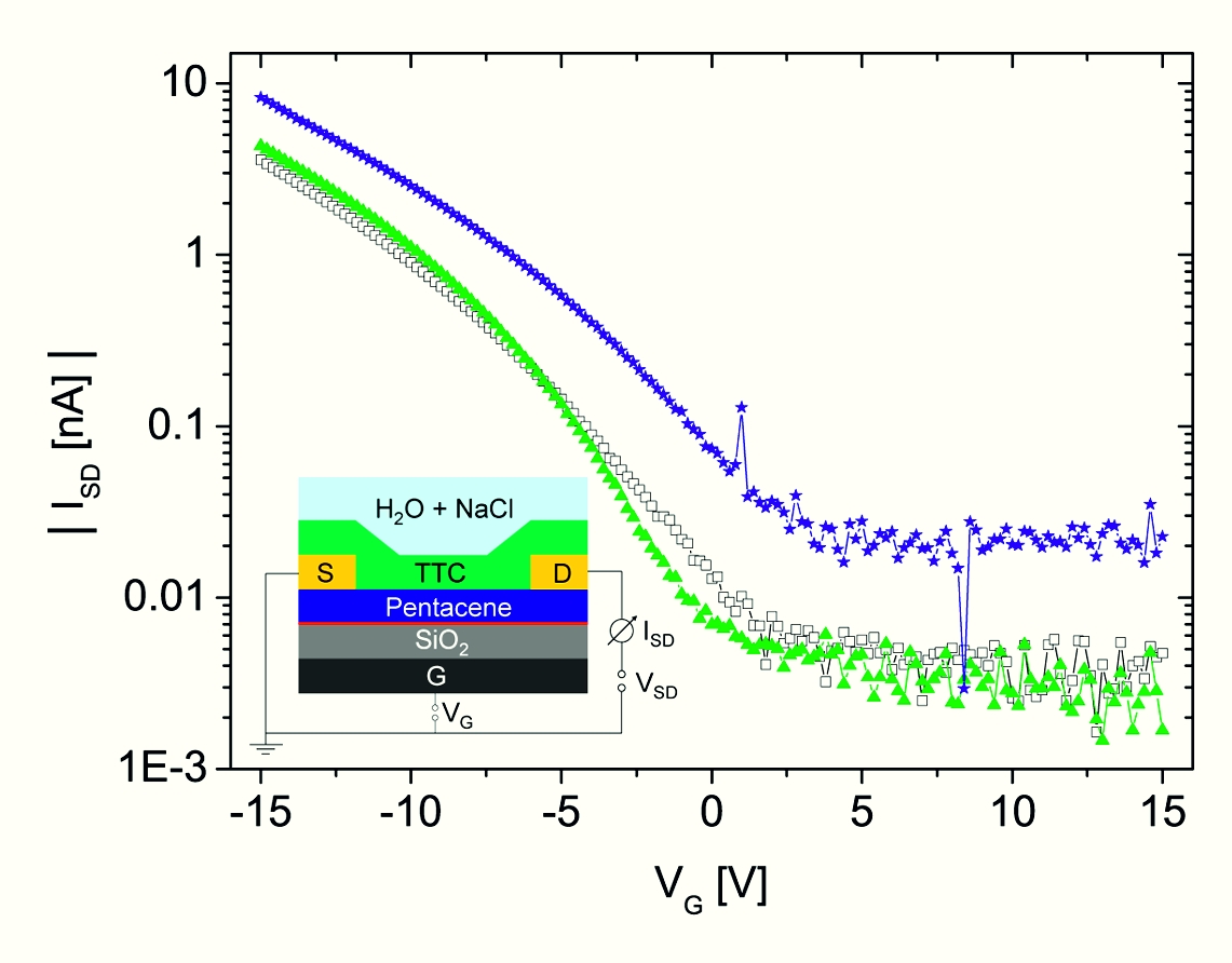
In the next step, we succeeded to show that a 50 nm TTC layer evaporated at optimized conditions on top of a pentacene thin-film transistor prevents degradation and ionic currents and thus allows for stable operation in a 1 mM NaCl solution over many hours. Compared to the operation in air, the transfer curves of the transistor immersed in buffer solution show only small changes, such as a slightly increased off-current and a voltage shift of 3.6 V (see Fig. 2). These effects can be explained by hole injection from the electrolyte into the pentacene film, i.e., the compensation of these additional holes requires a more positive gate voltage.
A biosensing device based on this setup might work on the principle of a double-gate transistor with floating top gate. In this case, the ratio of the bottom-gate and capping layer capacitance determines the sensitivity. Therefore, the small thickness of the TTC layer is the key for achieving the high sensitivity necessary for the readout of e.g. action potentials or DNA hybridization [3] in future developments.
| References | ||||||
|
| Contact information |
|
Bert Nickel E-Mail: nickel@lmu.de |
| Further Information |