


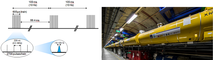
Figure 1: X-ray pulse repetition rate scheme, including the intra-train repetition rate of 4.5 MHz and the supercycle train repetition rate of 10 Hz (left), photograph of the accelerator modules of the European XFEL (right)
AGIPD was developed and tailored to the unique specifications of the European X-Ray Free Electron Laser (European XFEL) [1]. The European XFEL provides ultra-short, highly-intense, and highly-coherent X-ray pulses which will revolutionize scientific experiments in physics, chemistry, materials science, and biochemistry/biology.
One of the unique features of the European XFEL, compared to other XFELs, is the pulse repetition frequency and total number of X-ray pulses per second. At the European XFEL, X-ray pulses are delivered in bursts of so-called “pulse trains” with intra-train repetition rates as high as 4.5 MHz (pulse separation of by 220 ns). Each train consists of up to 2,700 pulses (total duration of entire train is 600 µs) and the repetition rate of trains is 10 Hz, resulting in a patterned pulse repetition rate scheme and up to 27,000 pulses/second.
The Adaptive Gain Integrating Pixel Detector (AGIPD) is one of the detectors developed specifically for the unique parameters of the European XFEL [2-11]. The development is a collaboration between DESY, the University of Hamburg, the University of Bonn and the Paul Scherrer Institute (PSI) in Switzerland.
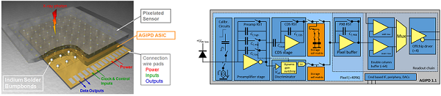
Figure 2: Conceptual design of a hybrid pixel array detector such as AGIPD (left) and schematic of the sensor (simplified as a diode, with “+UHV bias”) and AGIPD1.1 ASIC (right)
AGIPD is based on the hybrid pixel technology, with a sensor bump-bonded to the read-out chip (Application Specific Integrated Circuit - ASIC). AGIPD will feature p+-pixels of 200 µm x 200 µm size, fabricated on n-type silicon with a sensor thickness of 500 µm. To prevent charge spreading and insufficient charge collection from the sensor caused by plasma effects, which are expected at the high XFEL intensities [12, 13], operating at a bias voltage above 500 V is advisable, which, for X-ray radiation doses of up to 1 GGy, required a special optimization [14-16].
The newly developed AGIPD ASIC [3-11] works in hole-collecting mode. It utilizes a dynamic gain switching amplifier in each pixel, resulting in three distinct gain levels (high/medium/low gain), depending on the incoming signal. Single photon sensitivity [17] is ensured in the highest gain, while the medium and ultimately low gain mode provide a dynamic range of more than 104 12.4 keV photons. In order to cope with the 4.5 MHz repetition rate during the pulse train, images are temporarily stored in an analog memory of 352 memory cells per pixel; the data is read out from the memory cells in the 99.4 ms between pulse trains and digitized outside of the ASIC in external electronics on PCBs. An external veto signal, capable of overwriting any image previously recorded during the pulse train, can be provided during the pulse train in order to maximize the number of useful images from the up to 2,700 X-ray pulses/train to be stored in the 352 memory cells. The latest version of the ASIC is AGIPD1.2.
Current Status and Future Developments (as of 2019)
Currently, two 1Mpixel (1024 x 1024 pixel) AGIPD detector systems have been delivered to the SPB/SFX and MID Scientific Instruments of the European XFEL, commissioned and used for user experiments since 2017 (SPB/SFX) and 2018 (MID) respectively, resulting in high-impact publications.
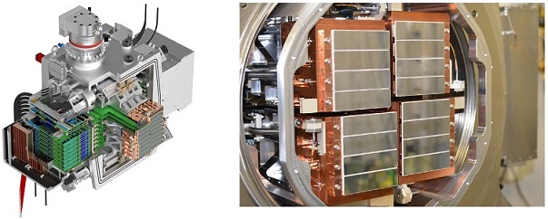
The AGIPD systems for SPB/SFX and MID feature a mechanical design comprised of four quadrants, each 512 x 512 pixels in size, which allow for adjustable geometries according to the needs of the respective experiments, especially if small-angle data is of particular importance. These systems are equipped with AGIPD1.1 ASICs.
A new version of the ASIC, AGIPD1.2, has been developed. The production of those ASICs has been concluded and new Front-End Modules (FEMs), comprised of sensor and ASICs are assembled. After testing and commissioning, the new FEMs will be given to XFEL in order to exchange them for the currently-used FEMs equipped with AGIPD1.1 ASICs at SPB/SFX and MID.
Two completely new AGIPD detectors are currently being designed for the European XFEL, one 4Mpixel AGIPD as a second detector for the SPB/SFX instrument, one 1Mpixel detector for the HED Instrument. These detectors will be equipped with new readout electronics including all-optical data transmission, a new FPGA, new firmware, and AGIPD1.2 FEMs.
As HED utilizes photon energies in the range of 20-30 keV, at which the quantum efficiency of 500- µm-silicon sensors is small, new high-Z materials such as Gallium-Arsenide (GaAs) and/or Cadmium-Telluride (CdTe) are investigated to be used as sensors [18-22]. For these sensors, a new ecAGIPD (electron-collecting AGIPD) is developed and a prototype is currently being tested. Initially, the HED AGIPD will be delivered with front-end modules equipped with silicon sensors which will eventually be upgraded to modules equipped with high-Z sensors.
Project Leader: Heinz Graafsma