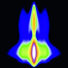
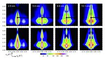
Figure 1: Composite image of four selected scattering images taken after deposition of a gold film with a thickness of 2.5, 5.6, 8.8 and 15.1 nm (upper row) and the corresponding simulations (lower row). The evolving maxima in vertical direction originate from the growth in height, the lateral maximum is related to the centre-to-centre distance of the clusters.
(Reprinted with permission from ACS Appl. Mat. Interfaces 1, 353 (2009). © 2009 American Chemical Society.)
Gunar Kaune1, Matthias A. Ruderer1, Ezzeldin Metwalli1, Weinan Wang1, Sebastien Couet2, Kai Schlage2, Ralf Röhlsberger2, Stephan V. Roth2, Peter Müller-Buschbaum1
1. Physik-Department E13, Technische Universität München, James-Franck-Straße 1, D-85747 Garching, Germany
2. HASYLAB at DESY, Notkestraße 85, D-22607 Hamburg, Germany
Published as: “In situ GISAXS study of gold film growth on conducting polymer films”, ACS Applied Materials and Interfaces 1, 353–362 (2009).
Almost all applications using conducting polymers require a metal contact. In a typical device, the interface between the polymer and the metal layer is of importance. Here we observe how a gold contact is formed on the conducting polymer polyvinylcarbazole (PVK) during sputter deposition. This growth process was observed in-situ via grazing incidence small-angle X-ray scattering (GISAXS). The GISAXS data were simulated with a cluster model, from which cluster morphology and arrangement were extracted. According to this model the growth proceeds in four steps where each stage is dominated by a characteristic kinetic process:
Nucleation is followed by lateral cluster growth, then coarsening occurs and finally a continuous layer grows in thickness. In addition to the contact formation, gold is incorporated inside the PVK film near the interface to the metal layer.
The field of organic electronics is emerging very rapidly, and newly-discovered materials and interfacial processes result in fascinating new applications. In these applications typically a thin metal film is used to apply an electrical contact to the active layer of an electronic device, e.g. an organic light emitting diode (OLED), an organic field effect transistor (OFET) or an organic solar cell (OSC). In a typical preparation procedure the metal film is deposited directly on top of the active layer, which corresponds to the introduction of an interface with the organic material in the device layout. Of rapidly growing interest is the class of conductive polymers, because they are easily processable by wet-chemical methods like spin coating. Moreover, conducting polymers can be tuned chemically and physically to meet the desired properties [1]. Independent from the polymer and metal used, an important concern in an organic electronic device are the interactions occurring at the polymer-metal interface, because characteristics like film adhesion and electric contact properties are strongly influenced by the interface structure and the incorporation of metal inside the polymer film. This in turn is determined by the growth of the metal film on the polymer surface, which makes a detailed understanding of the principles governing the growth process necessary.
Of particular interest for applications in organic electronic devices are polymers based on carbazole, because these polymers are characterized by high thermal and chemical stability and a low HOMO energy level [2]. For our investigation we prepared a 10 nm thick film of polyvinylcarbazole (PVK) and deposited a gold film on top of it by DC magnetron sputtering [3]. The film growth was monitored in-situ via grazing incidence small angle X-ray scattering (GISAXS) [4]. To achieve time resolution the experiment was performed in a stop-sputtering mode. In other words, cycles of gold deposition for 1 minute and subsequent recording of the GISAXS image were carried out. In total, 49 deposition cycles were done while a 15.1 nm thick gold layer was deposited. Afterwards the scattering images were simulated with a cluster model. Figure 1 shows a comparison of four selected scattering images and the corresponding simulations.
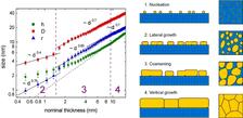
These simulations delivered the key parameters cluster radius r, height h and distance D to describe the evolution of the cluster morphology with the deposited film thickness (Figure 2). For the cluster height, a nonlinear progress with the deposited gold amount is obvious: Up to a value of 9 nm the cluster height exceeds the film thickness, which indicates a growth of the gold film in the form of three-dimensional, spherical clusters in the early stage of deposition. Over the whole deposition the cluster radius as well as the centre-to-centre distance of the clusters increase constantly with the deposited gold amount, indicating a cluster growth with permanent coalescence. Three distinct growth regimes with different scaling laws are observed. When complete surface coverage is reached at a nominal film thickness of d = 9nm the scaling law for the radius r shows a second transition to an identical scaling as the cluster distance. This progress of the cluster morphology suggests a cluster growth proceeding in four stages, with a characteristic kinetic process dominating each stage. The growth process begins with a stage of nucleation, where impinging gold atoms diffuse across the polymer surface and form nuclei when two of them meet. In the second stage, these nuclei grow laterally by capturing further diffusing atoms. As a result, small spherical gold clusters form. At a point where two clusters come in close contact to each other coalescence occurs and a larger cluster is formed. At a layer thickness of 1.3 nm enhanced coalescence sets in, cluster radius as well cluster distance increase very fast and the clusters start to assume an irregular shape (coarsening stage). In the final stage, the clusters form a continuous layer, which grows vertically in thickness as long as deposition goes on. Simultaneously coarsening continues and a grain structure, as it is well-known for vapour-deposited thin films, develops.
In addition to the formation of the metal layer on the conducting polymer, metal atoms diffuse into the PVK. An amount of 6.5 wt% gold is incorporated up to a depth of 1.2 nm in the PVK film. Eventually, the gold contact has evolved from isolated islands to a closed layer, and the observation gave us more insight how a metal film forms on a polymer surface and which processes determine the final film structure.
| References | ||||||||
|
| Contact Information |
|
Peter Müller-Buschbaum |
| Further Information |


