


")
")
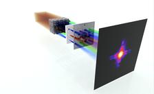
Scheme of the multibeam ptychography showing separation of the primary beam into individual beams which simultaneously irradiate multiple sample points. Scattered beams are recorded by the detector. (Credit: DESY, Mikhail Lyubomirskiy)
")
")
A newly developed X-ray imaging method can now visualise the internal structure of various samples, such as microchips or catalyst particles, with nanometre resolution over a large field of view without causing damage. This new technique, which was mainly developed at DESY´s high-brilliance X-ray source PETRA III, is of particular interest to the industry as a new characterisation method for R&D, as the developer team led by DESY scientist Mikhail Lyubomirskiy writes in the journal Advanced Science.
Unlike visible light, X-rays can penetrate matter to a great depth while providing spectacular resolution in the order of a few nanometres, thanks to a technique called ptychography. It works by scanning the sample in fine steps and recording how the X-rays get diffracted (scattered) by it. Ptychography can reach the highest resolution possible, but the step size while scanning has to be smaller than the diameter of the X-ray beam.
However, the penetration depth depends on the radiation wavelength:A shorter wavelength is required for a larger sample size. The sources of bright X-rays – synchrotron light sources – lose their generation efficiency as wavelength decreases, along with the fact that only a fraction of X-rays can be used, and the focusing efficiency of conventional X-ray optics reduces as well. PETRA III, which has the biggest circumference of all synchrotron radiation sources worldwide, can offer this technique at shorter wavelengths than other X-ray sources. However, it becomes extremely difficult to perform imaging experiments with shorter wavelengths, causing the measurement time to increase dramatically. One way to solve this problem is to upgrade to a new source with a more focused beam, but this problem will only shift towards shorter wavelengths as the general trend remains.
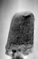
Another approach that the authors used, is what they call Multibeam Ptychography. An array of six to twelve nano lenses printed in a high-definition 3D printer brings a manifold beam of the synchrotron source on the sample, thus taking a larger fraction of incoming X-rays while still illuminating it with X-rays with a very short wavelength. Such a method can be particularly interesting in the microelectronics industry as it can deliver 3D visualisation of a whole microchip with resolution down to the transistor level. Or in the chemical industry, particularly in catalysis research and materials design.
For the application of the new technology, the team had to overcome two main challenges: creating optics that can be densely packed and still provide sufficient focusing power to spread X-rays over a large area at the detector without saturating it and separating signals from many different parallel beams.
“Our new approach combined the development of revolutionary optics manufactured by cutting-edge 3D printing technology, enabling parallel irradiation of thick samples with X-rays with very short wavelength (up to 0,06 nanometres) while maintaining sufficient focusing power and smart algorithms capable of disentangling signals from 12 parallel beams. For demonstration, we measured a microchip area of 120 x 90 micrometres using 12 parallel beams and a catalytic particle using 6 parallel beams, taking just under 10 minutes for each sample. The resulting images had a resolution of 38 nanometres. This way, we outperformed PETRA III state-of-the-art imaging beamline P06 by a factor of 12”, says Lyubomirskiy.
Currently, the team is developing this new Multibeam Ptychography to perform at even shorter wavelengths, shorter than 0,05 nanometres and with a larger number of parallel beams, which will enable routine imaging of large industrial-sized complex samples such as whole microchips or industrial catalysts. Combined with current and future 4th generation synchrotron radiation sources, especially DESY´s planned high-performance 3D X-ray microscope PETRA IV, this method will supersede single illumination imaging for studying large complex or composite samples.
This work is the result of the first year of a four-year project supported by the Röntgen Ångström Cluster (RÅC), a Swedish-German science collaboration. The project is dedicated to establishing this method at PETRA III and MAX IV facilities.
(from DESY News)
Reference:
X-Ray Multibeam Ptychography at up to 20 keV: Nano-Lithography Enhances X-Ray Nano-Imaging, Tang Li, Maik Kahnt, Thomas L. Sheppard, Runqing Yang, Ken V. Falch, Roman Zvagelsky, Pablo Villanueva-Perez, Martin Wegener, Mikhail Lyubomirskiy. Advanced Science (2024). DOI: 10.1002/advs.202310075