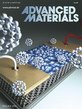
The 3D graphic on the right, created by NIM, shows the only nanometer sized object and induced the release of the publication as cover article (Credit: Advanced material, authors and NIM).
In solar cells and other semiconductor based devices electrons and electron holes have to move freely. Scientists from the Nanosystem Initiative Munich (NIM) have investigated its transport during production of ultra-thin organic conductor structures. The GISAXS measurements, in combination with other structural investigation methods like AFM, were performed at beamline W1 at DESY. The results were featured on the cover of 'Advanced Material'.
What do an espresso machine and a semiconductor have in common? Within both, tiny particles navigate through a complex maze. Steam has to penetrate the coffee powder at exactly the right pressure, while in semiconductors charge carriers have to find their way from electrode to electrode as easy as possible. Scientist call the existence of such a connected pathway from a source to its drain percolation. The group of NIM-physicist Bert Nickel (LMU Munich) is engaged in the study of such percolation phenomena in organic transistors.
Delayed transport
Their current publication in the journal Advanced Materials presents charge transport of electrons and holes through ultrathin organic layers during their deposition processes. In the scope of their experiment the scientists begin with the fabrication of a hole conducting layer which consists of small aromatic molecules (pentacene). After finishing this first layer, a second molecule is deposited on top. These molecules are football shaped, consisting of 60 carbon atoms (C60-fullerene or „Buckyballs“), and form an electron conducting film (cf. image). The research team expected percolation for electron flow after depositing only a single monolayer of C60. However, it took six layers of C60 molecules, until a corresponding electrical current could be observed. Taking a look at the surface with an atomic force microscope revealed that C60 forms small three dimensional droplets on the pentacene layer preventing the formation of connected paths from source to drain.
Floating Islands
The respective charging of the hole and the electron conducting layer upon contact can be tracked via gate voltage modulation. It was a surprise that this charging could only be observed after percolation. This leads to the assumption that the fullerene islands are potential-free before percolation.
Ambipolar components, i.e. electronic structures capable of conducting electrons and holes are key elements of organic solar cells. Such devices will benefit from the insights of the presented NIM research on percolation.
(News from Nanosystem Initiative Munich)
Reference:
Dual Channel Operation Upon n-Channel Percolation in a Pentacene-C60 Ambipolar Organic Thin Film Transistor. Simon J. Noever, Stefan Fischer, Bert Nickel. Advanced Materials, Volume 25, Issue 15, pages 2147–2151, April 18, 2013. DOI: 10.1002/adma.201203964


