


")
")
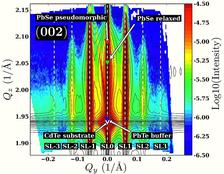
Figure 1: The left and right panel show the (002) and (115) reciprocal space maps around the CdTe Bragg position. Experimental data is denoted by the colour map while the black contour lines show the simulation data for a FWHM of 0.8 nm for the Gaussian inter-dislocation distance distribution.
E. Wintersberger1,3, N. Hrauda1, D. Kriegner1, M. Keplinger1, G. Springholz1, J. Stangl1, G. Bauer1, J. Oswald2, T. Belytschko2, C. Deiter3, F. Bertram3, O. H. Seeck3
1. Department of Semiconductor Physics, University of Linz, A-4040 Linz, Austria
2. Theoretical and Applied Mechanics, Northwestern University, 2145 Sheridan Road, Evanston, Illinois 60208-3111, USA
3. HASYLAB, DESY, Notkestrasse 85, D-22607 Hamburg, Germany
Published as: “Analysis of periodic dislocation networks using x-ray diffraction and extended finite element modeling”, Appl. Phys. Lett. 96, 131905 (2010).
Self organization provides a possibility to create dislocation free regions in heteroepitaxial semiconductor structures in order to improve the quality of subsequently grown devices. In this work the statistical properties of a periodic array of dislocations in thin PbSe films deposited on a PbTe buffer were investigated by means of X-ray diffraction. A novel method for the calculation of the displacement field due to the dislocations was used in order to circumvent the limitations of analytical solutions. A short range order model was applied successfully for the description of the dislocation distribution and verified by computer simulations.
Heteroepitaxial systems, consisting of materials with different lattice parameters, play a crucial role in the production of semiconductor devices. The strain induced by the lattice mismatch can be used to enhance the carrier mobility in electrically active layers [1]. However, once a layer exceeds a certain critical thickness the strain induced by the lattice mismatch is released by the formation of dislocations [2,3]. This process is referred to as plastic relaxation. The strain field produced by the dislocations influences the carrier mobility in subsequently grown active layers. Furthermore, the threading segments of the dislocations, penetrating these active layers contain dangling bonds and, therefore, act as electrically active scattering centres for the charge carriers, additionally reducing their mobility [4]. Therefore, the characterization of the dislocation distribution in such systems is an important step in the process optimization.
X-ray diffraction (XRD) usually probes a large volume of the sample and is therefore a well suited technique to investigate the average dislocation distribution within the scattering volume. From the position of the Bragg peak associated with a certain layer, the strain state and therefore the average density of dislocations can be obtained. For more detailed information about the dislocations the diffusely scattered intensity around this peak must be investigated which has been studied already by many groups [5,6]. However, these works are based on analytical formulas for the displacement field produced by dislocations and are thus limited to simple dislocation geometries and isotropic media. In this work we used a novel Finite Element Method (FEM) to overcome these limitations.
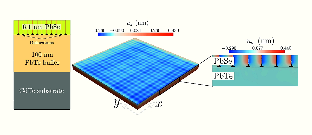
We investigate the statistical properties of a periodic dislocation network in a thin PbSe (6.1 nm thick) film on a 100 nm PbTe buffer. The buffer layer was deposited on a CdTe substrate. Both layers were grown by means of molecular beam epitaxy at a growth temperature of 360°C. The diffraction experiments were carried out at the new beamline P08 at PETRA III. In a coplanar diffraction geometry, reciprocal space maps (RSMs) were recorded around the (002) and (115) CdTe Bragg positions at an X-ray energy of 8994 eV. The colour maps in Fig. 1 show the (002) and the (115) RSMs recorded during the experiment. From the position of the PbSe peak in the (002) RSM it follows that the PbSe film is completely relaxed and therefore, plastic relaxation has occurred. Furthermore, the experimental data showed evidence that the dislocation distribution can be described by a short range order model (SRO) [7]. In such a model, the inter dislocation distance is described by a Gaussian distribution. From the evaluation of the RSMs a mean dislocation distance of 10.5 nm was found along with a FWHM of 0.81 nm of the underlying Gaussian distribution. These results raise two questions: (i) are there any other defects, which may contribute to the diffuse scattering and, (ii) what is the dominating type of dislocation in the sample?
In order to answer these questions, computer simulations of the diffusely scattered intensity were performed. The displacement field produced by the dislocations was calculated by means of the extended finite element method (XFEM). XFEM was introduced by Belytschko and Black [8] and applied to dislocations by Gracie [9].
Only pure edge dislocations with a Burgers vector parallel to the PbSe/PbTe interface are considered in our XFEM model (see Fig. 2). The dislocations are distributed by means of a random number generator so that the inter dislocation distance follows a Gaussian distribution with a mean value of 10.5 nm (as found in the experiment). The fitting variable for the simulations was the FWHM value of this Gaussian distribution. To obtain the diffraction pattern, the intensities of 20 XFEM domains were averaged for each FWHM value. Comparing the simulated data with the experimental data we found a best fit for a FWHM value of 0.8 nm for the simulations, which is close to the value we found in the experimental data. From the simulations the following conclusions can be made: (i) the dislocation distribution can be described with a SRO model, (ii) since we were able to reproduce the diffraction pattern with a single dislocation type, this type is the dominating type within the sample. The latter result is also reasonable from a physical point of view: the chosen type of dislocation is the most effective one for relieving strain. Finally, we have shown that the XFEM model is an applicable tool for the calculation of the displacement field produced by dislocations.
| References | ||||||||||||||||||
|
| Contact information |
|
Eugen Wintersberger |
| Further Information |