


")
")
Orbital texture within an atomic layer of 1T-TaS2, as obtained by state-of-the-art density functional theory. (Credit: Authors)
")
")
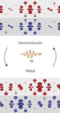
An international team of scientists from IFW Dresden, TU-Dresden, EPFL Lausanne (Switzerland), University of Illinois (US) and DESY found that the reordering of orbitals can cause a semiconductor to metal transition in nanostructures made of transition metal dichalcogenides. These orbital effects also provide an explanation for the recently discovered photoinduced semiconductor to metal transition in the transition metal dichalcogenide 1T-TaS2, indicating that these transitions can be triggered on ultrafast timescales.
The results have been obtained by combining X-ray diffraction at DESY’s light source DORIS III with photoemission done at BESSY in Berlin, and band structure calculations performed at the IFW in Dresden. The authors present their findings in the journal “Nature Physics”.
The transition metal dichalcogenides realize layered crystal structures, which make it easy to prepare them in thin-film form –an extremely advantageous feature for nanotechnology. This layered structure also causes a strongly anisotropic, quasi two-dimensional electronic structure. The latter in turn strongly favors electronic ordering instabilities and, in fact, the transition metal dichalcogenides are well known to exhibit an instability against the formation of so-called charge density waves (CDW), i.e, a crystallization of mobile electrons in the two-dimensional layers.
Correspondingly, most of the previous research focused essentially isolated two-dimensional layers. However, drastic changes of the X-ray diffraction pattern of the CDW measured at the DORIS III beamline BW5, revealed that this may not be sufficient and that correlations between layers need also to be considered. Indeed the electronic structure calculations uncovered complex orbital textures (see figure), which are interwoven with the CDW order and cause dramatic differences in the electronic structure depending on the alignment of the orbitals between neighboring planes.
The new twist of the paper is the discovery that these orbital-mediated interactions may enable to drive semiconductor to metal transitions with technologically pertinent gaps and on ultrafast timescales. This opens up new routes to fabricate optically switchable devices based on orbitally textured CDW compounds, a new technology that could be called "Orbitronics".
These discoveries are hence of special relevance for the ongoing development of novel, miniaturized and ultrafast devices for electronic and sensing applications. They also enable to explain a number of long-standing puzzles associated with the electronic self-organization in 1T-TaS2: the ultrafast response to optical excitations, the high sensitivity to pressure and a mysterious commensurate phase that is commonly thought to be a special phase (‘Mott phase’) and that is not found in any other isostructural modification.
Charge density wave states have recently also been observed in a large number of cuprate high-Tc superconductors and their relation to other phases like the pseudo gap, the anti-ferro magnetic phase and superconductivity is currently under debate. To elucidate the role played by the orbital degree of freedom for superconductivity will be another challenge.
(from authors)
Publication:
„Orbital textures and charge density waves in transition metal dichalcogenides“, T. Ritschel, J. Trinckauf, K. Koepernik, B. Büchner, M. v. Zimmermann, H. Berger, Y. I. Joe, P. Abbamonte and J. Geck, Nature Physics (2015), DOI: 10.1038/nphys3267